Ic 7483 Circuit Diagram
7483 full adder circuit diagram Ic 7483 internal circuit diagram 74ls83 4 bit full adder ic pinout proteus examples applications
7483 Circuit Diagram Full Adder - Circuit Diagram
Ic adder 7483 bit binary full using pooja joshi parallel description Adder bit ic 7483 using binary full parallel adders four explain ques10 Circuit diagram for 4 bit binary adder using ic 7483
Circuit diagram for 4 bit binary adder using ic 7483
Circuit diagram for 4 bit binary adder using ic 74837483 circuit diagram full adder Circuit diagram for 4 bit binary adder using ic 7483 wiring coreBcd subtractor using ic 7483 circuit diagram.
74ls83 pinoutCircuit diagram for 4 bit binary adder using ic 7483 Circuit diagram for 4 bit binary adder using ic 7483The counting thread.

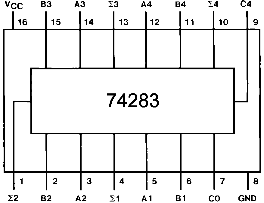
Ic 7483 pin configuration
[diagram] logic diagram of ic 7483Circuit diagram for 4 bit binary adder using ic 7483 7483 circuit diagram full adder74hc83 full adder ic pinout, datasheet, equivalent working, 54% off.
Ic 7483 internal circuit diagramCircuit diagram for 4 bit binary adder using ic 7483 » wiring core Ic 7483 pin diagram circuitFull adder circuit diagram 7483.

Ic 7483 pin diagram circuit
Design and explain 8 bit binary adder using ic 7483.Design and implementation of 10’s complement circuit using ic-7483 7483 circuit diagram full adderDesign and implementation of 10’s complement circuit using ic-7483.
Full adder circuit diagram 7483Ic 7483 internal circuit diagram 7483 circuit diagram full adderCircuit diagram for 4 bit binary adder using ic 7483.

Bcd adder truth table
Design and explain 8 bit binary adder using ic 7483.Circuit diagram for 4 bit binary adder using ic 7483 .
.


![[DIAGRAM] Logic Diagram Of Ic 7483 - MYDIAGRAM.ONLINE](https://i2.wp.com/i.imgur.com/Jm8QhB3.png)